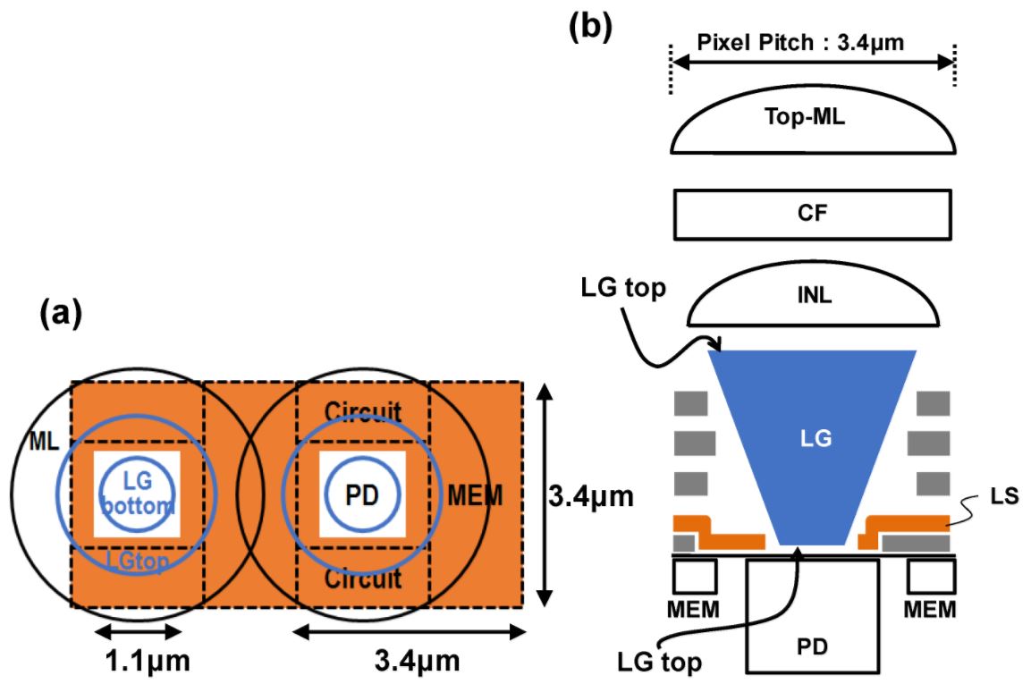
"CISs with GS function have generally been inferior to the rolling shutter (RS) CIS in performance, because they have more components. This problem is remarkable in small pixel pitch. The newly developed 3.4 µm pitch GS CIS solves this problem by using multiple accumulation shutter technology and the gentle slope light guide structure. As a result, the developed GS pixel achieves 1.8 e− temporal noise and 16,200 e− full well capacity with charge domain memory in 120 fps operation. The sensitivity and parasitic light sensitivity are 28,000 e−/lx·s and −89 dB, respectively. Moreover, the incident light angle dependence of sensitivity and parasitic light sensitivity are improved by the gentle slope light guide structure."


Could this light guide approach be seen as a 'poor man's BSI'? Because it increases the fill factor without going for a more complex processing (as required for BSI).
ReplyDeleteAs I understand it, BSI would not bring you much advantage because a memory area is needed beside the photo diode. (And the memory area is twice the size of the photo diode.)
ReplyDeleteI assumed, that for BSI with global shutter the memory area would also be placed on the backside (don't know though if that would be possible as I am no expert).
DeleteMore in general for non-global shutter sensors: I am wondering if the taper could be Canon's building block to achieve similar performance per pixel as BSI but with a simpler process.
If I understand this correct, they do two transfers from the photo diode to the memory area per frame? I think, this is only really useful if the time between the two transfers is half of the desired total exposure time (in contrast to half the frame time - e.g. you could want 1ms exposure time at 60fps). After taking a quick look at the paper, it was not clear to me if this is the case.
ReplyDeleteI dont know if it is similar but it sounds at least similar in Sony pregius - they call it 'multi exposure' and there it seems the add charge to a charge domain storage multiple times before readout. I also thought it could act as a 'tuneable grey filter' reducing sensitivity (this is sometimes desired if you have a lot of light, sometimes this is a problem in industrial applications). You might want to expose over 20ms periode but only 100us every 2ms - reducing sensitivity to 5% while maintaining the 20ms that might also "filter" higher frequency vibration.
ReplyDeleteThis raises two questions: a) what kind of tricks are theoretically possible with this pixel (e.g. I am not sure if your "grey filter" works as you have to be able to get rid of the charge between the small exposure periods) and b) what is supported by the readout circuits of the respective products
Delete